Nanofabrication
We use state-of-the-art clean room facilities available in-house to fabricate various types of nanoscale devices. These devices are utilized for a range of electronic transport measurements, including scanning photocurrent microscopy (SPCM), spin transport experiments and magnetotransport studies, all of which are carried out between room temperature and 300 mK.
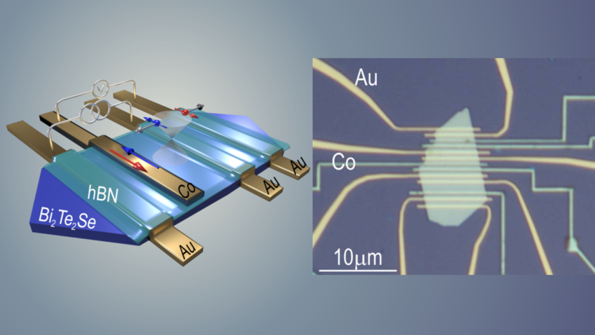
As a major nanofabrication method, e-beam lithography is employed using a standard two-layer PMMA resist system to obtain electrodes with widths as low as 50 nm. The nanostructured electrodes are typically defined in two- or four-probe configuration on top of individual nanostructures such as graphene flakes/stripes, or sheets composed of a 2D quantum material (3D topological insulators or Weyl semimetals). Besides the conventional back gate configuration, we implement top gate electrodes separated from the underlying nanostructure by an ultrathin alumina or titania film deposited by atomic layer deposition (ALD). Furthermore, prior to metal evaporation the contact areas are often cleaned by an in situ argon plasma treatment, in order to achieve the best possible cleanliness of the interface between contact metal and material.