Resolving Magnetic Properties at Atomic Scale
The development of atomic-scale quantitative magnetic characterization techniques promises further progress in nanotechnology, such as the development of high density data storage. A reliable method to perform magnetism measurement at such high spatial resolution is the experimental technique based on electron magnetic circular dichroism (EMCD) in a transmission electron microscope (TEM) – a method first developed by Prof Schattschneider et al. in 2003 [1,2]. Recently, an attractive technique using an astigmatic electron probe within a Cs-corrected scanning transmission electron microscope (STEM) has been proposed by Jan Rusz et al. [3], theoretically showing great potential for measuring EMCD with atomic resolution. Their calculation reveals that it is possible to obtain the EMCD signal at the transmitted beam directly without the necessity of producing electron vortex beams. The key feature is the relation between the crystal structure, the magnetic symmetry of the sample, and the distribution of the phase in the electron beam. A certain amount of aberration should be introduced to obtain the required phase symmetry of the electron beam and to measure the non-zero EMCD signal in the transmitted beam. This magnetic signal reaches its maximum intensity when the beam is passing directly through an atomic column and drops dramatically when the beam is away from the center. Practically, by simply taking the difference of in-column and off-column spectra, or of different atomic columns with opposite magnetic moments (in anti-ferromagnetic materials), the EMCD signal can be extracted at atomic scale.
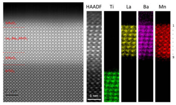
In our work, we aim to obtain the EMCD signal with atomic resolution experimentally. The work is firstly carried out on La0.7Ba0.3MnO3 ferromagnetic thin films where the magnetism is provided by Mn. Since the properties of perovskite materials are closely related to their structures, preliminary STEM research is being carried out using a JEOL ARM200F in the aberration-corrected condition to gain insight into the structural and chemical nature of the thin films. STEM-HAADF images show no structural defects in the perovskite SRO/LBMO/SRO multilayer heterostructures. Atomically resolved EELS-based elemental maps of Ti, La, Ba, Mn, acquired across the thin film, reveal a sharp non-diffusing interface between LBMO and the neighboring SRO layers. The Mn electronic structure is probed across the LBMO layer by means of high-energy resolved ELNES at the Mn L2,3 edges. The ELNES spectra extracted from the interfaces show the same features as the ones within the layer, indicating a well-defined homogenous chemical structure for Mn. These STEM findings can explain the good magnetic properties of LBMO at such low thickness. In the future, EELS spectrum images with sub-Å pixel size will be recorded under an asymmetric probe condition together with accurate measurements of the aberrations, which is expected to provide a reliable and explainable EMCD signal.
[1] C. Hebert, P. Schattschneider, Ultramicroscopy 96 (2003) 463-468.
[2] P. Schattschneider, S. Rubino, C. Hebert, et al., Nature 441 (2006) 486.
[3] Jan Rusz, Juan-Carlos Idrobo and Somnath Bhowmick, PRL 113 (2014) 145501.
Researchers from the Nanoscale Functional Heterostructures research group in Dept. Mannhart collaborate in this project.


