When stacking and intercalation synergize
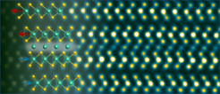
Electron microscopy of Nb1+xSe2 reveals layer-by-layer contrasts between 180º-stacked NbSe2 layers heavily intercalated with excess Nb and 0º-stacked NbSe2 layers with few Nb intercalants.
One reason that layered, two-dimensional (2D), van der Waals materials have been so successful over the past two decades is that their interlayer coupling hits a “sweet spot”. The interaction between the layers is weak enough that the individual layers can be considered quasi-2D and are easy to exfoliate or intercalate. However, the interaction is also strong enough that stacking the layers with different in-plane shifts and rotations can strongly change their electronic properties. An entire research industry has been built around mechanically exfoliating 2D materials with Scotch tape and then intricately re-stacking them in new ways to fabricate heterostructures. To make such systems scalable, one wonders whether it is possible to grow 2D materials epitaxially with deterministic control over the stacking orientation at each layer.
It turns out that certain transition metal dichalcogenides (TMDCs) have given us a chemical tuning knob to control their stacking orientation. The well-known charge-density-wave superconductor NbSe2 adopts a so-called 2Ha stacking polytype, in which successive layers of NbSe2 are stacked with 180º in-plane rotation. When synthesized with a few percent of excess Nb, Nb1+xSe2 self-intercalates and transforms into the 3R polytype with 0º stacking of layers. With increasing x, polycrystalline samples of Nb1+xSe2 have shown a mixture of intercalated stacking polytypes, but without a local probe, it is difficult to clarify what is happening at the microscopic level.

Foreground: crystal structure of Nb1+xSe2. The arrows mark the in-plane orientations of each layer. Nb intercalants are predominantly found in the van der Waals gap of 180°-stacked layers, while leaving the van der Waals gap of the 0°-stacked layers relatively empty.
Wang et al. use scanning transmission electron microscopy to bring a new pair of eyes to the old art of intercalated TMDCs. In epitaxial thin films of Nb1+xSe2, x ≈ 0.3, the authors observe a nanoscale phase mixture of 180º- and 0º-stacked NbSe2 layers. The 180º-stacked layers are heavily intercalated with Nb on the order of tens of percent occupancy, but the 0º-stacked layers are nearly empty with few detectable intercalants. The contrast is so robust that the stacking orientation could be abruptly changed from 180º to 0º in a given layer of the film, and immediately the van der Waals gaps change from being heavily intercalated to being nearly empty.
Several microscopic factors are responsible for this observation. While previous reports have found a stacking rotation from 180º to 0º around x ≈ 0.03–0.07, our results imply a second stacking rotation from 0º back to 180º around x ≈ 0.3, which is close to the percolation threshold of the intercalants. Nb1+xSe2 also appears to undergo a phase separation (spinodal decomposition) around x ≈ 0.3, resulting in a nanoscale mixture of 180º-stacked layers with local x > 0.3 and 0º-stacked layers with local x < 0.3. Kinetic processes involved in the synthesis of the thin films may also play a role.
The real challenge now lies ahead: can stacking-selective self-intercalation be used as a scalable means to fabricate NbSe2 films with layer-by-layer control of stacking orientation? What kind of functionality can result from having atomically sharp junctions between 180º- and 0º-stacked layers?
This work was performed in the StEM group and the Quantum Materials Department in collaboration with the Interface Analysis, Crystal Growth, and Thin Film Technology groups, as well as with the Department of Materials and Geosciences at the TU Darmstadt.


