A touch of gold and silver
For the first time, it is possible to produce crystalline layers of precious metals that consist of a single atomic layer and which are semiconducting
Metals are usually characterized by good electrical conductivity. This applies in particular to gold and silver. However, researchers from the Max Planck Institute for Solid State Research in Stuttgart, together with partners in Pisa and Lund, have now discovered that some precious metals lose this property if they are thin enough. The extreme of a layer only one atom thick thus behaves like a semiconductor. This once again demonstrates that electrons behave differently in the two-dimensional layer of a material than in three-dimensional structures. The new properties could potentially lead to applications, for example in microelectronics and sensor technology.
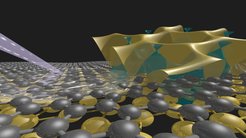
. The electronic structure of the gold layer and the graphene (green) is shown above. The Stuttgart Max Planck researchers spectroscopically determined the electronic properties by examining the sample with a photon beam (grey).")
One might think that gold leaf, which is only 0.1 µm thick, is actually quite thin. Far from it. It can actually be several hundred times thinner. For example, the research team of Ulrich Starke and his former doctoral student Stiven Forti have successfully created a gold layer only a single atom thick. Two-dimensional gold, so to speak.
Starke is head of the Interface Analysis Facility at the Max Planck Institute for Solid State Research in Stuttgart. His team has long been working on the border between three-dimensional (voluminous) and two-dimensional (planar) materials. Solid state researchers are interested in this transition because it is associated with changes in certain material properties. This has previously been demonstrated in two-dimensional carbon, or graphene. Among other things, its electrons are significantly more mobile and allow the electrical conductivity to increase to 30 times that of the related three-dimensional graphite.
Gold atoms are pushed between graphene and silicon carbide
However, for many metals, producing layers of material just one atom thick is not an easy task. “With classical deposition methods, gold atoms, for example, would immediately agglomerate into three-dimensional clusters”, explains Starke. His team is therefore working with a different method – intercalation – on which they did pioneering work around 10 years ago. Intercalation literally means sliding something in between. And that is precisely how it works. The researchers start with a silicon carbide wafer. Using a process they developed themselves, they first convert its surface into a single-atomic layer of graphene. “If we vaporise sublimated gold on to this silicon carbide-graphene arrangement in a high vacuum, the gold atoms migrate between the carbide and the graphene”, explains Forti. The former Max Planck doctoral candidate is now doing research at the Center for Nanotechnology Innovation in Pisa. It is not yet fully understood how the thick gold atoms get into the interstitial space. But this much is clear: higher temperatures favour the process.
The team had also applied the intercalation technique to other elements, including germanium, copper, and gadolinium. Yet, according to Forti, the main focus was the influence on the properties of graphene. In the case of gold, however, it was found for the first time that the intercalated atoms arranged themselves in a regular, periodically recurring two-dimensional structure – crystalline – along the silicon carbide surface. “If the intercalation is carried out at 600°C, the graphene layer prevents the gold atoms from agglomerating to form drops”, says Forti about the function of the carbon layer in the sandwich structure.
A gold layer consisting of only two atomic layers conducts like a metal
The successful preparation of the gold layer of one atom thickness was only the first step. Subsequently, the extremely thin materials and their possibly special characteristics became interesting for the researchers. They could indeed show that the extremely thin layer of gold develops its own electronic – and semiconductor – properties. To compare: the electrical conductivity of voluminous (i.e. three-dimensional gold) is nearly as good as that of copper. Because theoretical considerations forecast a metallic character for pure 2D gold, the semiconductor finding was somewhat surprising. “Interactions between the gold atoms and either the silicon carbide or the graphene carbon obviously still play a role here. This influences the energy levels of the electrons”, says Starke.
Semiconductors are essential materials in microelectronics and other fields. For example, electronic switching elements such as diodes or transistors are based on it. Starke’s team can envisage some typical semiconductor applications for the new 2D material. A second layer of gold atoms again gives a metallic character – and thus influences the electrical conductivity. “By varying the amount of sublimated gold, we can tightly control whether one or two layers of gold form”, explains Forti.
It would therefore be conceivable to use components with alternating single- or double-atomic gold layers. The new manufacturing method would then have to be suitably combined with common lithographic methods of chip production. For example, diodes significantly smaller than conventional ones could be produced. According to Starke, the different electronic states of single and double-layer gold could also be used in optical sensors.
Electronic effects also in the graphene layer

Another application idea results from effects caused by the intercalated gold in the adjacent graphene layer, which apparently depend on the thickness of the gold. “A gold layer one atom thick causes an n-doping in the graphene. This means we obtain electrons as charge carriers”, says Forti. In spots where the gold is two atomic layers thick, exactly the opposite – p-doping – happens. There, missing electrons or positively charged so-called “holes” act as charge carriers. The gold also enhances the interaction of plasmons (i.e. fluctuations in the density of charge carriers) with electromagnetic radiation. “A structured, alternating arrangement of n- and p-doping in the graphene could thus be used. For example, as a highly sensitive yet high-resolution detector array for terahertz radiation like those used in materials testing, for security checks at airports, or for wireless data transmission”, says Starke.
Starke’s team has already taken the next step in the production of two-dimensional precious metal layers. Also in an intercalation experiment with silver, a strictly crystalline two-dimensional silver layer formed between silicon carbide and graphene. And what’s more: even this metal, which is usually an even better electrical conductor than gold, becomes a semiconductor when reduced to two dimensions. The initial results indicate that the energy required to make the silver layer electrically conductive is probably higher than for 2D gold. “The semiconductor properties of a component made from this material might therefore be thermally more stable than those of gold”, says Starke about possible practical consequences.
KH