2D materials
WS2 and WSe2 layers were grown on epitaxial graphene on SiC(0001) establishing a defined epitaxial relationship between substrate and transition metal dichalcogenide (TMD) layer. Large scale ordered TMD layers could be obtained with a dense coverage of domains aligned with a high percentage. The preferred rotational order parallel to the graphene lattice is manifested by the emergence of TMD related spots in the LEED patterns.
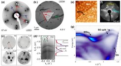
Two different approaches were chosen for preparing the TMD layers: WS2 layers were grown in a conventional chemical vapor deposition (CVD) process in an ex-situ furnace (in collaboration with the group of C. Coletti (IIT, Pisa) (Forti 2017). For WSe2 we used a novel UHV based hybrid growth process combining MBE and pulsed laser deposition (PLD) (Nakamura, 2020). This hybrid growth technique was first established for growth on sapphire substrates (Mohammed 2017). CVD grown WS2 reaches an island size of several μm, while the hybrid process for WSe2 results in islands on a 100 nm scale. Yet, here, on monolayer graphene even a coalescence of the islands is approaching. LEED and X-ray diffraction (XRD) demonstrate the successful epitaxial alignment of individual seeds in both cases. ARPES experiments resolve the band dispersion for both TMD systems with high energy resolution. In particular, for WS2, the experiment (ARPES and μ-ARPES) shows a record split value of the spin-orbit splitting as compared to other experimental results (Forti 2017). A clear cross-influence effect on the electronic structure is observed as seen by the changed band alignment on different substrates (SiC, EG), as well as the hole doping appearing in the EG layer (Nakamura 2020), indicating the possibility of engineering the proximity influence.
-(d) WS2 on graphene on SiC(0001); (e)-(g) WSe2 on graphene on SiC(0001)")
This research is in colaboration with the Takagi department, the Kern department and the Center for Nanotechnology Innovation @ NEST, Istituto Italiano di Tecnologia in Pisa.
Publications:
- H. Nakamura, A. Mohammed, Ph. Rosenzweig, K. Matsuda, K. Nowakowski, K. Küster, P. Wochner, S. Ibrahimkutty, U. Wedig, H. Hussain, J. Rawle, C. Nicklin, B. Stuhlhofer, G. Cristiani, G. Logvenov, H. Takagi, U. Starke, Phys. Rev. B 101, 165103 (2020). Spin splitting and strain in epitaxial monolayer WSe2 on graphene.
- A. Mohammed, H. Nakamura, P. Wochner, S. Ibrahimkutty, A. Schulz, K. Müller, U. Starke, B. Stuhlhofer, G. Cristiani, G. Logvenov, and H. Takagi, Appl. Phys. Lett. 111, 073101 (2017). Pulsed laser deposition for the synthesis of monolayer WSe2.
- S. Forti, A. Rossi, H. Büch, T. Cavallucci, F. Bisio, A. Sala, T.O. Mentes, A. Locatelli, M. Magnozzi, M. Canepa, K. Müller, S. Link, U. Starke, V. Tozzini, and C. Coletti, Nanoscale 9, 16412-16419 (2017). Electronic properties of single-layer tungsten disulfide on epitaxial graphene on silicon carbide.