2D semiconducting van der Waals interface layers
 FS with Dirac cone and Au-bands, (b) 2D-Au band dispersion, togetherwith TB-simulations (red), (c) spin-orbit splitting of the 2D-Au bands.")
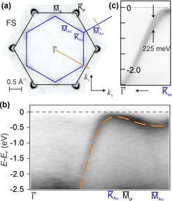
with TB-simulations (red), (c) spin-orbit splitting of the 2D-Au bands.
Another strong advantage of the use of SiC over metal substrates is that also the intercalant might be decoupled from the substrate and its electronic properties can be investigated individually with only little interference of the semiconducting substrate. For example, we could recently show that 2-dimensional gold constrained in-between graphene and SiC is a semiconductor - in contrast to its bulk metallic behaviour. The valence band maximum resides 50 meV below the Fermi level exhibiting a significant Rashba type band splitting of 225 meV along the ΓK direction of the Au layers' Brillouin zone (Forti 2020). By tuning the amount of gold a semiconductor to metal transition of the 2D gold layer can be introduced. The intercalation of silver leads to a similar semiconducting 2D layer while its maximum valence band resides 590 meV below the Fermi level (Rosenzweig and Starke 2020). The band dispersion of both system can be modeled with a simple tight binding calculation confirming the weak interaction of the semiconducting layers with the SiC substrate and the graphene. Being graphene-encapsulated, these Au and Ag intercalation systems also define a novel type of van der Waals (vdW) heterostructure.
Publications:
- P. Rosenzweig, U. Starke, Phys. Rev. B 101, 201407(R) (2020). Large-area synthesis of a semiconducting silver monolayer via intercalation of epitaxial graphene.
- S. Forti, S. Link, A. Stöhr, Y. Niu, A. A. Zakharov, C. Coletti, U. Starke, Nat. Commun. 11, 2236 (2020). Semiconductor to metal transition in two-dimensional gold and its van der Waals heterostack with graphene.