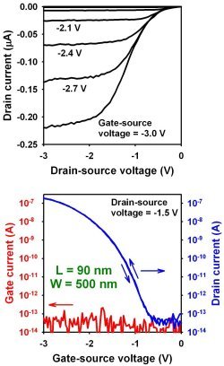
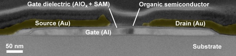
| As the channel length of organic thin-film transistors (TFTs) is reduced into the micron or submicron regime in order to improve the dynamic TFT performance, the total resistance and the transconductance of the TFTs become more and more limited by the contact resistance, rather than by the channel resistance. To better understand the properties of organic TFTs with very small channel length and to explore ways to alleviate the contact resistance effects in aggressively scaled organic TFTs, we have developed a method to prepare organic TFTs with lithographically patterned metal gate electrodes, a thin gate dielectric based on an oxygen-plasma-grown metal oxide and an alkylphosphonic acid self-assembled monolayer (SAM), and source/drain contacts patterned by electron-beam lithography on the surface of the organic semiconductor. Owing to the small thickness of the gate dielectric, TFTs with a channel length as short as 100 nm display a pronounced saturation of the drain current, along with a large on/off current ratio (close to 107) and a steep subthreshold swing (150 mV/decade). In addition, we have found that the introduction of a strong molecular dopant (NDP-9; developed by Novaled) into the contact regions of the TFTs leads to a significant reduction of the contact resistance, so that the desirable linear behavior in the output characteristics at small drain-source voltages is recovered. |
 |
|
 |
||
Contact Doping and Ultrathin Gate Dielectrics for Nanoscale Organic Thin-Film Transistors
F. Ante, D. Kälblein, U. Zschieschang, T. W. Canzler, A. Werner, K. Takimiya, M. Ikeda, T. Sekitani, T. Someya, H. Klauk
Small, vol. 7, no. 9, pp. 1186-1191, May 2011