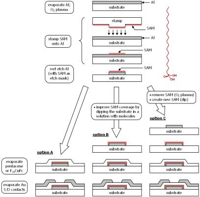
| Printing techniques developed for organic electronics are usually either direct or indirect, i.e. the printed layer is either a functional material that becomes part of the final device, or it is a resist that serves as a mask during a subtractive or additive patterning step. We have developed a manufacturing process for organic thin-film transistors that combines the concepts of direct and indirect printing in the same printing step and for the same material, by employing a microcontact-printed self-assembled monolayer first as an etch resist to define the metal gate electrode of an organic transistor, and then as the gate dielectric of the final device. |
 |
|
 |
||
High-resolution spatial control of the threshold voltage of organic transistors by microcontact printing of alkyl and fluoroalkylphosphonic acid self-assembled monolayers
I. Hirata, U. Zschieschang, T. Yokota, K. Kuribara, M. Kaltenbrunner, H. Klauk, T. Sekitani, T. Someya
Organic Electronics, vol. 26, pp. 239-244, November 2015
Spatial control of the threshold voltage of low-voltage organic transistors by microcontact printing of alkyl- and fluoroalkyl-phosphonic acids
I. Hirata, U. Zschieschang, F. Ante, T. Yokota, K. Kuribara, T. Yamamoto, K. Takimiya, M. Ikeda, H. Kuwabara, H. Klauk, T. Sekitani, T. Someya
MRS Communications, vol. 1, no. 1, pp. 33-36, November 2011
Microcontact-Printed Self-Assembled Monolayers as Ultrathin Gate Dielectrics in Organic Thin-Film Transistors and Complementary Circuits
U. Zschieschang, M. Halik, H. Klauk
Langmuir, vol. 24, no. 5, pp. 1665-1669, February 2008